
Swinburne’s Space Technology and Industry Institute combines internationally competitive capabilities from advanced manufacturing, space science, artificial intelligence, and resource processing to tackle challenges at the forefront of human understanding and imagination.
The institute contributes and propels innovation and economic growth in a global sector projected to be worth $1 trillion by 2040. It fosters education at every level, from vocational training to PhD.

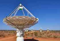
Swinburne's space technology capabilities
Learn more about space technology at Swinburne and how we are paving the way by combining our globally renowned capabilities in astrophysics, aerospace, aviation, engineering, advanced manufacturing, and digital technologies.
Our research
The Space Technology and Industry Institute collaborates with future-focussed industry partners to identify needs, design solutions and develop technologies in a range of fields central to the space sector.
Our people
Our team comprises experts in aerospace technology, and next-generation design and manufacturing.
Space science and technology courses
School-leavers, current students and professionals can all find courses to propel them into the next generation of space technology innovators. Explore our range of courses today.
-
Space Technology
When you study space technology at Swinburne, you'll explore the most exciting topics in space science, such as: microgravity science, space environment, and space entrepreneurship.
-

Robotics and Mechatronics Engineering
Swinburne's Robotics and Mechatronics Engineering courses equip you with advanced systems design skills spanning mechanical, electronic and software engineering. -

Youth Space Innovation Challenge
Secondary students can design and lead an experiment that blasts off to the International Space Station each year through the Swinburne Youth Space Innovation Challenge.


Work with us
We have a talented group of scientists and engineers with a broad range of expertise across space technology – we can work with you to drive innovation and help solve your complex problems.
-
Get in touch
Tell us your challenges, ideas or big questions, and we’ll work with you to share our expertise. Call us on +61 3 9214 5177 or email spaceinstitute@swinburne.edu.au.
-
Come together
Relevant experts from our team will work with you to create ideas and identify possible solutions to the challenges we are facing.
-
Resource
If the project needs funding, that is something we can tackle together with various opportunities to explore.
-
Find the solutions
We design and implement a research project to address the issues at hand and deliver innovative, achievable solutions.
Fungi experiment blasts off
An experiment spearheaded by Swinburne's astrophysicists Dr Sara Webb and Dr Rebecca Allen has blasted off to space containing three species of fungi - Lion’s Mane, Turkey’s Tail and Cordyceps. Designed, tested, and built with the assistance of high school students from Haileybury College, the project aims to understand how funghi can support astronaut health for long-duration space missions.
Harvesting metal from the moon
PhD candidate, Matthew Shaw from the Space Institute took home first place prize and the peoples’ choice award at the 2021 Virtual Asia-Pacific 3MT Final where his presentation Lunacy on the production of metal on the Moon stood up against 7 other finalists from Australia, New Zealand, Japan, Hong Kong, Malaysia and Singapore.
Space junk
Astronomy Professor Alan Duffy discusses how Australia’s helping to fight the snowballing threat of space junk. Swinburne University and partners are engaging in a project called ‘Responsible AI in Space’, a collaboration between space scientists, law and policy experts, the space industry, government and practitioners in the emerging field of AI assurance.
Engagement and highlights

The Swinburne Space Technology and Industry Institute team and invited guests.
Space Technology and Industry Institute Showcase
Held 2 March 2023, this showcase highlighted the work of Swinburne’s Space Technology and Industry Institute and the partnerships it has forged with industry leading organisations. The event was hosted by founding Institute Director Professor Alan Duffy, with Swinburne Chief Scientist Professor Virginia Kilborn welcoming delegates and partners.
Featured speakers included Dr Timo Stuffler, Director of Business Development at OHB System AG in Munich, and Ms Lynette Tan, Chief Executive at Singapore Space & Technology Ltd; and panels comprising leading industry professionals shared details of cutting-edge research.
The showcase saw wonderful engagement and feedback from participants, highlighting critical skills and challenges to assist in focusing the institute’s strategy. There was positive interaction between staff, colleagues and industry partners, with networking opportunities for research professionals.
Our latest news
-
- Astronomy
- Science
- University
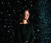
Swinburne astrophysicist makes Forbes 30 under 30 Asia list
Swinburne astrophysicist and science communicator Dr Kirsten Banks has made the Forbes 30 under 30 Asia list for social media, marketing and advertising
Friday 29 May 2026 -
- University
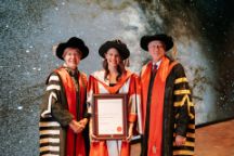
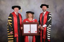
Swinburne recognises Australian space innovator with Honorary Doctorate
Swinburne University of Technology has recognised Katherine Bennell-Pegg, a trailblazer in space engineering and exploration, with an Honorary Doctorate of the University.
Friday 08 May 2026 -
- Astronomy
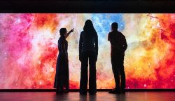
One of the world’s most ambitious 3D immersive LED screens, the Virtual Universe, launches at Swinburne
Swinburne's Virtual Universe is opening at Swinburne University of Technology for public and undergraduate education
Thursday 30 April 2026 -
- University
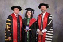
Swinburne recognises space innovator with Honorary Doctorate
Swinburne University of Technology has recognised Anousheh Ansari, a trailblazer in space engineering and exploration, with an Honorary Doctorate in Science.
Friday 17 April 2026 -
- Student News
- Technology
- Science
- University
Swinburne awards 2025 University Medals to outstanding students
From cutting‑edge science and technology to world‑leading research, three Swinburne students from the School of Science, Computing and Emerging Technologies have been recognised with the prestigious 2025 University Medal
Thursday 16 April 2026


Discover our other research institutes
Subscribe to our mailing list
Keep up to date with the latest news and events from the Space Technology and Industry Institute.
By signing up, you consent to MailChimp collecting your data, which is treated in accordance with Swinburne's Privacy Statement. You can unsubscribe at any time.Contact the Space Technology and Industry Institute
If your organisation would like to collaborate with us to solve a complex problem, or you simply want to contact our team, get in touch by calling +61 3 9214 8180 or emailing spaceinstitute@swinburne.edu.au.